www.yw193,五月天婷婷网站,国产美女裸身网站免费观看视频,内射干少妇亚洲69XXX,妞干网成人,少妇中文字幕乱码亚洲影视,国产精品国产三级国产专播,国产99久60在线视频%20|%20传媒
      myMaker - Events - Chinese Version
      Search Product, Company or News
      Home > Electronic Components & Supplies > Semiconductor Material > Fused Silica Wafers
      Edmund Optics Inc. (EO) logo
      Edmund Optics Inc. (EO)
      Company  |  Products  |  News  |  Contact Us
      Fused Silica Wafers
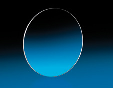
      UV Fused Silica Substrate
      Ultrasonically Cleaned
      Less than 10Å Surface Roughness

      Fused Silica Wafers are thin, circular pieces of UV fused silica designed to be used as test substrates to measure the quality of optical coatings. Fused Silica Wafers have been ultrasonically cleaned and are delivered in contaminant-free packaging to ensure quality. Additionally, these optical wafers can also be used as dummy components for set-up processes or for semiconductor, microlithography, or micro electro-optical applications (MEMS).

      Related Products
      Silicon
      Jiangxi LDK Solar Hi-Tech Co., Ltd.
      Production Technologies We use metallurgical silicon as a raw material to produce TCS, which is then used to produce polysilicon. This technology enables ...

      Semiconductor Material Exhibitions
      Global Semiconductor Hub 2026
      3/17/2026 - 3/19/2026
      Phoenix AZ, United States
      CSTIC 2026
      3/22/2026 - 3/23/2026
      Shanghai, China
      Electronic Materials Conference (EMC) 2026
      6/24/2026 - 6/26/2026
      Detroit MI, United States
      ESSERC 2026
      9/7/2026 - 9/10/2026
      Palma, Spain
      SEDEX 2026
      10/14/2026 - 10/16/2026
      Seoul, South Korea
      More Trade Shows


      About newMaker | Gold Suppliers | Contact Us | showsbee.com | showseye.com | newMaker China | My newMaker  
      © newMaker.com. All Rights Reserved